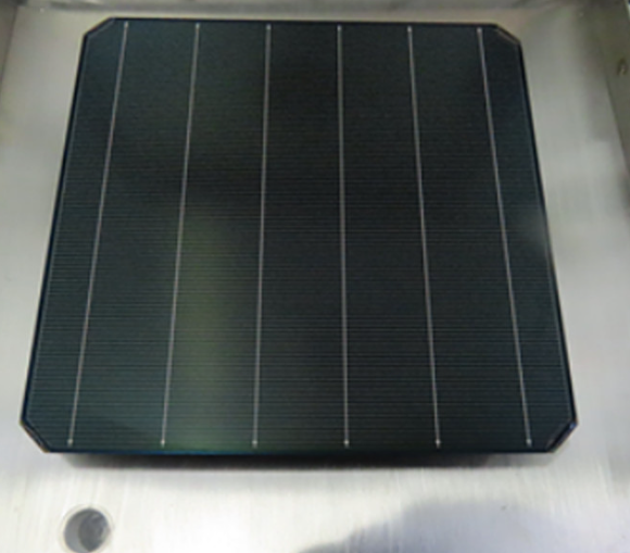
The device combines passivated tunneling contacts with dielectric passivation layers and integrates both n-type and p-type contacts on the rear surface. Key features include a high-resistivity half-cut M10 wafer with edge passivation, an optimized n-type contact created through a high-low temperature process, an indium tin oxide (ITO) layer for lateral carrier transport, and a multilayer front-surface stack of aluminum oxide and silicon nitride for reduced recombination.
The team significantly lowered phosphorus doping in the n-type polycrystalline silicon layer to minimize dopant diffusion. They also introduced in situ passivated edge technology (iPET), which passivates wafer edges during fabrication. Deep 8-micrometer trenched metal fingers collect holes, while selective ITO etching prevents leakage between contact types. An enhanced amorphous silicon layer fully encapsulates the structure, and pulsed green nanosecond laser crystallization reduces contact resistivity without compromising edge passivation.
The certified 27.81% efficiency was achieved on a cell with an active area of 133.63 cm², delivering a short-circuit current of 5,698 mA, open-circuit voltage of 744.9 mV, and fill factor of 87.55%. The exceptionally high fill factor results from an ideality factor below 1 at maximum power point, made possible by advanced laser-induced crystallization, in situ edge passivation, and optimized surface treatments.
Longi stated that the new techniques are compatible with existing heterojunction (HJT) production lines and can be scaled for commercial manufacturing. The company noted that further reduction in p-type contact resistivity remains a priority for continued efficiency gains.
The breakthrough demonstrates simultaneous advances in optical management and carrier transport, establishing a new benchmark for crystalline silicon photovoltaic technology while maintaining compatibility with large-scale industrial processes.

